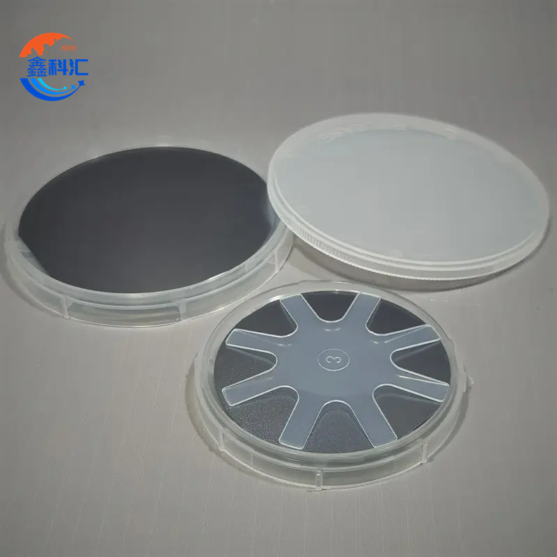
Li-wafer tsa Indium Antimonide (InSb) mofuta oa N mofuta oa P Epi e se e loketse ho se etsoe Li-wafer tsa Te tse nang le dope kapa Ge tse nang le dope Botenya ba 2inch 3inch 4inch Indium Antimonide (InSb)


Likaroloana
Dikgetho tsa ho sebelisa lithethefatsi:
1. E phutholotsoe:Li-wafer tsena ha li na metsoako efe kapa efe ea doping, e leng se etsang hore li be ntle bakeng sa lits'ebetso tse khethehileng tse kang kholo ea epitaxial.
2.Te Doped (N-Mofuta):Ho sebelisa lithethefatsi tsa Tellurium (Te) hangata ho sebelisoa ho etsa li-wafer tsa mofuta oa N, tse loketseng lits'ebetso tse kang li-infrared detector le lisebelisoa tsa elektroniki tse lebelo le phahameng.
3.Ge Doped (P-Type):Ho sebelisa doping ea Germanium (Ge) ho sebelisetsoa ho etsa li-wafer tsa mofuta oa P, tse fanang ka ho tsamaea ha masoba a maholo bakeng sa lits'ebetso tse tsoetseng pele tsa semiconductor.
Likhetho tsa Boholo:
1. E fumaneha ka bophara ba lisenthimithara tse 2, lisenthimithara tse 3, le lisenthimithara tse 4. Li-wafer tsena li khotsofatsa litlhoko tse fapaneng tsa theknoloji, ho tloha lipatlisisong le nts'etsopele ho isa tlhahisong e kholo.
2. Ho mamellana ha bophara bo nepahetseng ho netefatsa botsitso ho pholletsa le lihlopha, ka bophara ba 50.8±0.3mm (bakeng sa li-wafer tsa lisenthimithara tse 2) le 76.2±0.3mm (bakeng sa li-wafer tsa lisenthimithara tse 3).
Taolo ea Botenya:
1. Li-wafer li fumaneha ka botenya ba 500±5μm bakeng sa ts'ebetso e ntle lits'ebetsong tse fapaneng.
2. Litekanyo tse ling tse kang TTV (Total Thickness Variation), BOW, le Warp li laoloa ka hloko ho netefatsa hore li tšoana hantle ebile li na le boleng bo holimo.
Boleng ba Bokaholimo:
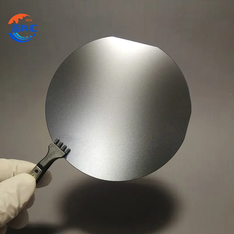
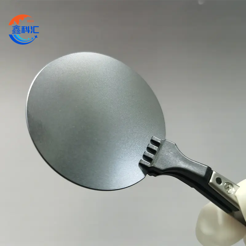
1. Li-wafer li tla le bokaholimo bo bentšitsoeng/bo bentšitsoeng bakeng sa ts'ebetso e ntlafalitsoeng ea mahlo le ea motlakase.
2. Libaka tsena li loketse kholo ea epitaxial, li fana ka motheo o boreleli bakeng sa ts'ebetso e tsoelang pele lisebelisoa tse sebetsang hantle.
E Loketse Epi:
1. Li-wafer tsa InSb li loketse ho sebelisoa epi, ho bolelang hore li phekotsoe esale pele bakeng sa lits'ebetso tsa ho beoa ha epitaxial. Sena se etsa hore li be ntle bakeng sa ts'ebeliso tlhahisong ea semiconductor moo likarolo tsa epitaxial li hlokang ho lengoa holim'a wafer.
Likopo
1. Di-detector tsa infrared:Li-wafer tsa InSb li sebelisoa hangata ho lemoha infrared (IR), haholo-holo karolong ea infrared ea bolelele ba maqhubu a bohareng (MWIR). Li-wafer tsena li bohlokoa bakeng sa pono ea bosiu, litšoantšo tsa mocheso, le lits'ebetso tsa infrared spectroscopy.
2. Lisebelisoa tsa Elektroniki tse Potlakileng:Ka lebaka la ho tsamaea ha tsona ka dielektrone tse ngata, di-wafer tsa InSb di sebediswa disebedisweng tsa elektroniki tse lebelo le hodimo tse kang di-transistors tse nang le maqhubu a hodimo, disebediswa tsa quantum well, le di-transistors tse nang le motlakase o phahameng (HEMTs).
3. Lisebelisoa tsa Liliba tsa Quantum:Lekhalo le lesesaane la bandgap le motsamao o motle wa dielektrone di etsa hore di-wafer tsa InSb di lokele ho sebediswa disebedisweng tsa quantum well. Disebediswa tsena ke dikarolo tsa bohlokwa di-laser, di-detector, le ditsamaiso tse ding tsa optoelectronic.
4. Lisebelisoa tsa Spintronic:InSb e boetse e hlahlojoa lits'ebetsong tsa spintronic, moo ho potoloha ha electron ho sebelisetsoang ts'ebetso ea tlhahisoleseling. Khokahano e tlase ea spin-orbit ea thepa e etsa hore e be e loketseng lisebelisoa tsena tse sebetsang hantle.
5. Litšebeliso tsa Mahlaseli a Terahertz (THz):Disebediswa tse thehilweng ho InSb di sebediswa ditshebedisong tsa mahlaseli a THz, ho kenyeletswa le dipatlisiso tsa saense, ditshwantsho, le tlhaloso ya thepa. Di thusa mahlale a tswetseng pele jwalo ka ditsamaiso tsa ditshwantsho tsa THz le THz.
6. Lisebelisoa tsa Thermoelectric:Thepa e ikhethang ea InSb e etsa hore e be thepa e khahlang bakeng sa lits'ebetso tsa thermoelectric, moo e ka sebelisoang ho fetolela mocheso hore e be motlakase ka katleho, haholo-holo lits'ebetsong tse ikhethileng joalo ka theknoloji ea sebaka kapa tlhahiso ea motlakase libakeng tse feteletseng.
Liparamente tsa Sehlahisoa
| Paramethara | Li-inch tse 2 | Li-inch tse 3 | Li-inch tse 4 |
| Bophara | 50.8±0.3mm | 76.2±0.3mm | - |
| Botenya | 500±5μm | 650±5μm | - |
| Bokaholimo | E bentšitsoeng/E qapiloeng | E bentšitsoeng/E qapiloeng | E bentšitsoeng/E qapiloeng |
| Mofuta oa ho sebelisa lithethefatsi | E sa phutholohang, Te-doped (N), Ge-doped (P) | E sa phutholohang, Te-doped (N), Ge-doped (P) | E sa phutholohang, Te-doped (N), Ge-doped (P) |
| Boikutlo | (100) | (100) | (100) |
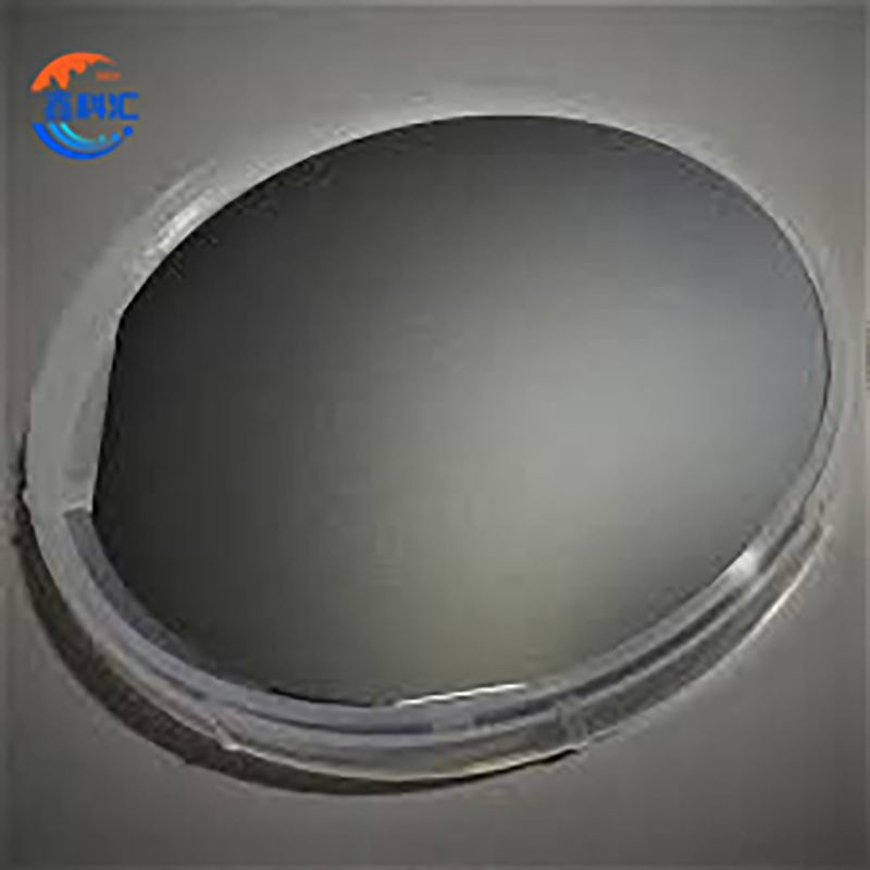
| Sephutheloana | E le 'Ngoe | E le 'Ngoe | E le 'Ngoe |
| E loketse Epi | E | E | E |
Liparamitha tsa Motlakase bakeng sa Te Doped (N-Type):
- Ho tsamaea: 2000-5000 cm²/V·s
- Ho hanyetsa: (1-1000) Ω·cm
- EPD (Botebo bo Phethahetseng): ≤2000 diphoso/cm²
Liparamitha tsa Motlakase bakeng sa Ge Doped (P-Type):
- Ho tsamaea: 4000-8000 cm²/V·s
- Ho hanyetsa: (0.5-5) Ω·cm
- EPD (Botebo bo Phethahetseng): ≤2000 diphoso/cm²
Qetello
Li-wafer tsa Indium Antimonide (InSb) ke thepa ea bohlokoa bakeng sa mefuta e mengata ea lits'ebetso tse sebetsang hantle masimong a lisebelisoa tsa elektroniki, li-optoelectronic le theknoloji ea infrared. Ka ho tsamaea ha tsona ka mokhoa o motle oa li-electron, ho kopanya ha tsona ka tsela e tlase ea spin-orbit, le likhetho tse fapaneng tsa doping (Te bakeng sa mofuta oa N, Ge bakeng sa mofuta oa P), li-wafer tsa InSb li loketse ho sebelisoa lisebelisoa tse kang li-infrared detectors, li-transistors tse lebelo le phahameng, lisebelisoa tsa quantum well, le lisebelisoa tsa spintronic.
Li-wafer li fumaneha ka boholo bo fapaneng (2-inch, 3-inch, le 4-inch), ka taolo e nepahetseng ea botenya le libaka tse loketseng ho kenngoa ka epi, ho netefatsa hore li fihlela litlhoko tse matla tsa tlhahiso ea semiconductor ea sejoale-joale. Li-wafer tsena li loketse lits'ebetso masimong a kang ho lemoha IR, lisebelisoa tsa elektroniki tse lebelo le phahameng, le mahlaseli a THz, ho nolofalletsa mahlale a tsoetseng pele lipatlisisong, indastering le ts'ireletsong.
Setšoantšo se qaqileng