Sekhahla sa teko sa Silicon sa lisenthimithara tse 4 FZ CZ N-Type DSP kapa SSP


Hlahisa lebokose la wafer
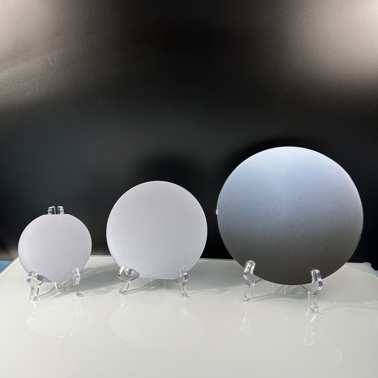
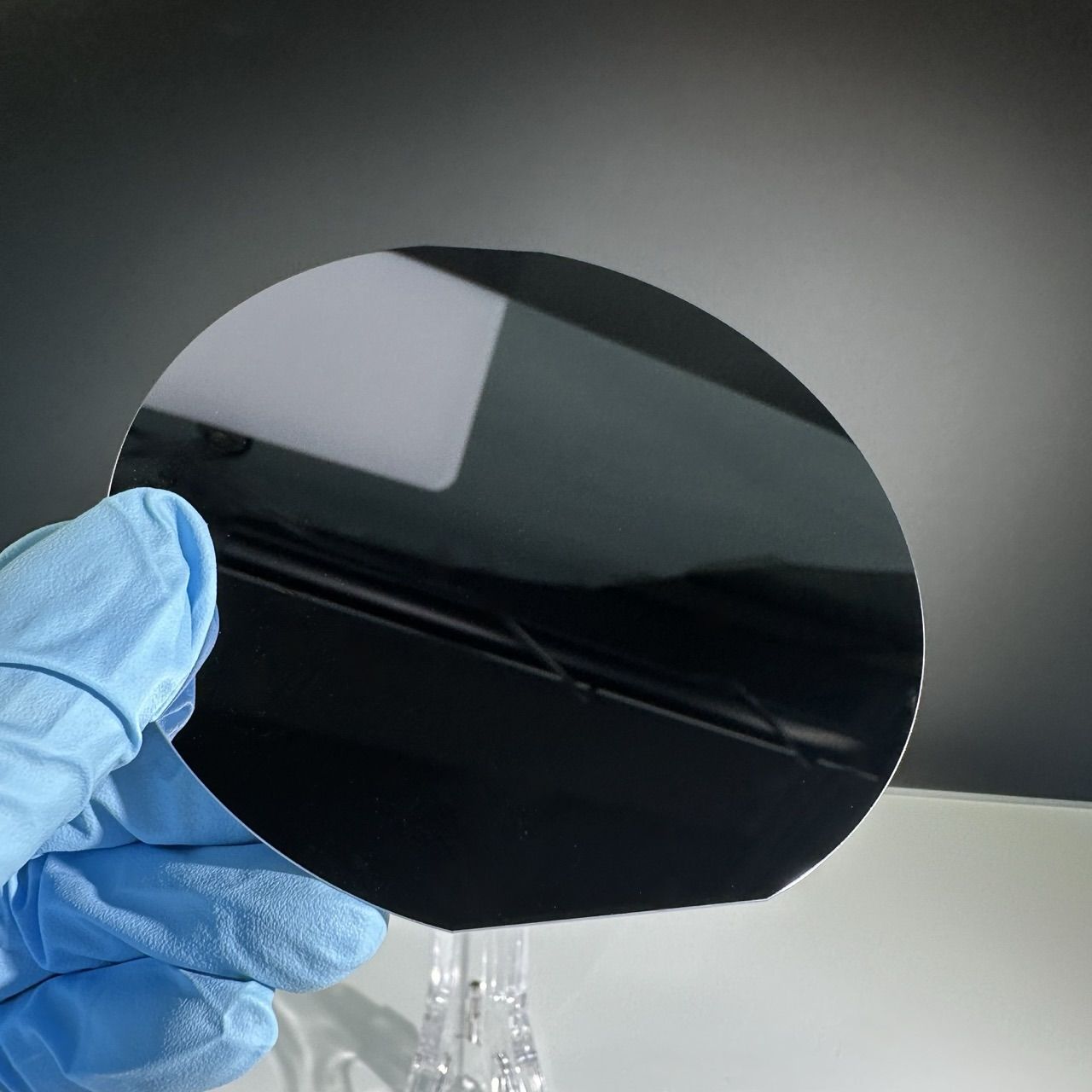
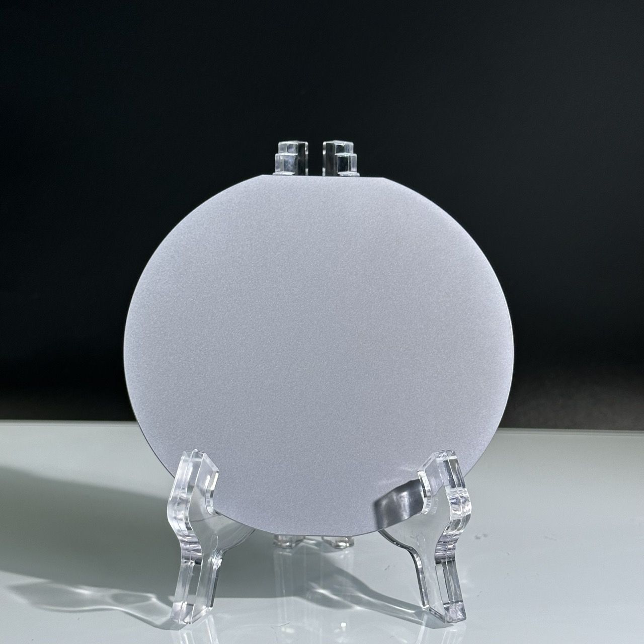
Li-wafer tsa silicon ke karolo ea bohlokoa ea lefapha la theknoloji le ntseng le hola kajeno. 'Maraka oa thepa ea semiconductor o hloka li-wafer tsa silicon tse nang le litlhaloso tse nepahetseng ho hlahisa palo e kholo ea lisebelisoa tse ncha tsa potoloho e kopaneng. Rea hlokomela hore ha litšenyehelo tsa tlhahiso ea li-semiconductor li ntse li eketseha, litšenyehelo tsa thepa eo ea tlhahiso, joalo ka li-wafer tsa silicon le tsona lia eketseha. Re utloisisa bohlokoa ba boleng le katleho ea litšenyehelo lihlahisoa tseo re li fang bareki ba rona. Re fana ka li-wafer tse theko e tlaase le tsa boleng bo tsitsitseng. Haholo-holo re hlahisa li-wafer tsa silicon le li-ingots (CZ), li-wafer tsa epitaxial, le li-wafer tsa SOI.
| Bophara | Bophara | E bentšitsoeng | E entsoe ka doped | Boikutlo | Ho hanyetsa/Ω.cm | Botenya/um |
| 2inch | 50.8±0.5mm | SSP DSP | P/N | 100 | 1-20 | 200-500 |
| 3inch | 76.2±0.5mm | SSP DSP | P/B | 100 | NA | 525±20 |
| 4inch | 101.6±0.2 101.6±0.3 101.6±0.4 | SSP DSP | P/N | 100 | 0.001-10 | 200-2000 |
| 6inch | 152.5±0.3 | SSPDSP | P/N | 100 | 1-10 | 500-650 |
| 8inch | 200±0.3 | DSPSSP | P/N | 100 | 0.1-20 | 625 |
Tšebeliso ea li-wafer tsa silicon
Substrate: Seaparo sa PECVD/LPCVD, ho phunya ha magnetron
Substrate: XRD, SEM, spectroscopy ea infrared ea matla a athomo, microscopy ea elektrone ea phetisetso, spectroscopy ea fluorescence le liteko tse ling tsa tlhahlobo, kholo ea epitaxial ea mahlaseli a limolek'hule, tlhahlobo ea X-ray ea ts'ebetso ea microstructure ea kristale: ho fata, ho kopanya, lisebelisoa tsa MEMS, lisebelisoa tsa motlakase, lisebelisoa tsa MOS le ts'ebetso e 'ngoe.
Ho tloha ka 2010, Shanghai XKH Material Tech. Co., Ltd e ikemiselitse ho fa bareki litharollo tse felletseng tsa Silicon Wafer ea wafer ea lisenthimithara tse 4, ho tloha ho li-wafer tsa boemo ba ho lokisa liphoso tsa Dummy Wafer, li-wafer tsa boemo ba teko Test Wafer, ho ea ho li-wafer tsa boemo ba sehlahisoa Prime Wafer, hammoho le li-wafer tse khethehileng, li-wafer tsa Oxide Oxide, li-wafer tsa Nitride Si3N4, li-wafer tse koahetsoeng ka aluminium, li-wafer tsa silicon tse koahetsoeng ka koporo, SOI Wafer, MEMS Glass, li-wafer tse entsoeng ka mokhoa o ikhethileng tse teteaneng haholo le tse bataletseng haholo, jj., tse nang le boholo bo tlohang ho 50mm-300mm, 'me re ka fana ka li-wafer tsa semiconductor ka ho bentša ka lehlakore le le leng/mahlakore a mabeli, ho tšesaane, ho arola, MEMS le lits'ebeletso tse ling tsa ts'ebetso le tsa ho iketsetsa.
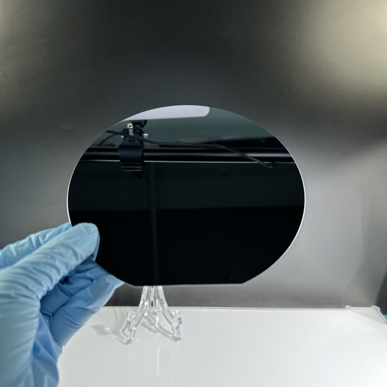
Setšoantšo se qaqileng
Lihlahisoa tse Amanang
-
Sekoahelo sa Silicon sa 4inch FZ CZ N-Type DSP kapa SSP Tes ...
-

2inch 50.8mm Silicon wafer FZ N-Type SSP
-
Wafer ea Silicon ea mofuta oa N kapa mofuta oa P ea lisenthimithara tse 6
-
Sepache sa Silicon sa 8inch P/N-mofuta (100) 1-100Ω dummy...
-
FZ CZ Si wafer e teng setokong sa 12inch Silicon wafer Pr ...